Skip to content

ASIC & VLSI Services

Aten provides Cutting-Edge Application-Specific Integrated Circuit (ASIC) and Very Large Scale Integration (VLSI) Design Services, enabling highly specialized and Optimized Hardware Solutions for demanding applications.

Custom AI/ML Accelerator Design​

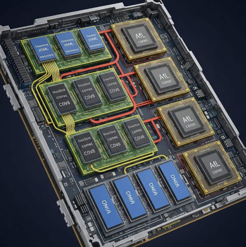
We Design Application-Specific Integrated Circuits (ASICs) specifically tailored for High-Performance, Power-Efficient AI/ML Inference at the edge. These Custom Chips enable Real-Time Data Analysis directly on UAVs and NanoSatellites, supporting Complex Neural Network Operations within strict Power Constraints.

Specialized Integrated Circuit (IC) Development

Our expertise lies in developing Custom ASICs for functions requiring Optimal Performance and minimal Power Consumption, such as Sensor Interfaces, Data Converters and Secure Communication Modules. This approach offers Superior Performance and IP Protection compared to Off-the-Shelf Components.

System-on-Chip (SoC) & IP Core Development

We offer End-to-End VLSI Design Services, including Architecture Definition, RTL Design and Verification, Physical Design and Tape-Out for Complex Systems-on-Chip (SoCs). These SoCs integrate multiple functionalities like Processors, Memory, Communication Interfaces and Sensor Hubs onto a single chip, crucial for Highly Integrated and Autonomous Platforms.
Physical Design & Verification

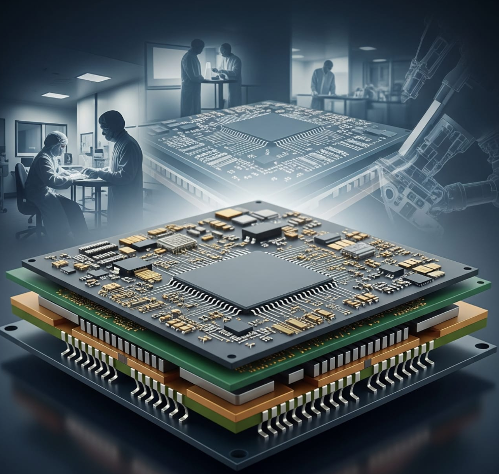
Our Services encompass the complete Physical Design Flow, including Floorplanning, Place and Route, Timing Closure and Power Optimization. We conduct rigorous Verification, including Functional, Formal and Timing Verification, to ensure the Design performs as intended and meets all Performance Requirements. 

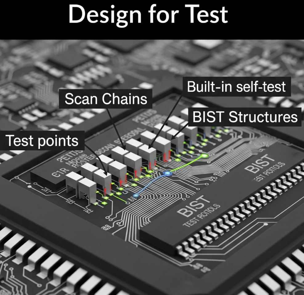
Design for Test (DFT)​​

We integrate Scalable Testability Features into our ASIC and VLSI Designs from conceptualization to ensure comprehensive and efficient Chip Testing. This enhances yield and facilitates Efficient Manufacturing, resulting in High-Quality, Fault-Tolerant Chips.